What is nanotechnology: simply about the complex. What is nanotechnology? Nanotechnology definition
Where is nanotechnology used? Nanotechnology in the modern world is used in many industries, and in which ones you will find out in this article. The Nanotechnology Report contains a lot of useful information.
Where are nanotechnologies used?
Achievements of nanotechnology are used in the following industries:
Application of nanotechnology in medicine: ensure acceleration of the development of new drugs, create highly effective forms and methods of delivering drugs to the site of the disease, offer new diagnostic tools, and allow non-traumatic operations
Nanotechnology began to be used in the production of fashionable clothing recently. Some of the fashion designers began collaborating with scientists to produce models of so-called “functional clothing”. It will differ from the one we are used to not only in appearance, but also in the properties of the fabric from which it is made.
Clothes made from carbon nanotubes do not require washing, it is impossible to get sick in them, they do not allow harmful gases to pass through and protect against modern ecology. 1 sq. A meter of fabric costs about 10 thousand. $
Application of nanotechnology in construction. Nanomaterials for construction, autonomous energy sources based on powerful solar panels, nanofilters for water and air purification - these achievements of nanotechnology should be made - and are already being done! — our homes have become more comfortable, more reliable, safer. Adding nanoparticles (including carbon nanotubes) to concrete makes it several times stronger. Nanocoatings are being developed to protect concrete structures from water. Steel, an essential building material, also becomes much stronger when vanadium and molybdenum nanoparticles are added. Self-cleaning glass with titanium dioxide nanoparticles is already being produced by industry. In the future, nanofilm glass coatings will optimally regulate the flow of light and heat through windows. To protect buildings from fire, nanotechnologies offer both new non-flammable materials (for example, cable insulation containing clay nanoparticles) and “smart” networks of ultra-sensitive nanofire sensors. Wallpaper coated with zinc oxide nanoparticles will help clean the room from bacteria. As for home appliances - refrigerators, televisions, plumbing fixtures, lighting fixtures, kitchen equipment - the field of applications for nanotechnology is inexhaustible.
Nanomaterials in industry At the moment, nanomaterials are the least toxic and most biocompatible with a living cell (human, plant, animal). Produced nanomaterials find high-quality application in almost any industry:
- fuel (fuel catalysts, increasing octane number, minimizing emissions);
- cosmetic (enrichment with microelements, bactericidal properties);
- textile, shoe (bactericidal and healing properties of clothing and shoes);
- paint and varnish (bactericidal varnishes and paints, special coatings);
- leather (antifungal treatment of skin);
- medical (new generation medications, nanovitamin complexes of microelements);
- in the agro-industrial complex (nanofertilizers, feed additives, product storage);
- food industry (dietary supplements, vitamin complexes);
- and also: pulp and paper, chemical, municipal, electronics, energy, mechanical engineering as an additional raw material component that imparts additional properties to products.
Application of nanotechnology in mechanical engineering
The automotive industry is one of those. that they are the first to perceive innovations, including nanotechnological ones. Already today, the global turnover of products using nanotechnology in this industry is estimated at more than $8 billion. Here are just a few examples of how nanoinnovations are transforming familiar elements of a car. Composite materials make it possible to make body parts strong and lightweight. Adding nanoparticles to fuel increases the efficiency of its combustion, while simultaneously reducing the amount of harmful substances emitted into the atmosphere. Nanoparticles found in oil help increase engine life: according to some data, the use of such additives reduces wear of parts by 1.5-2 times. Carbon nanoparticles (so-called black carbon) are added to tire rubber, and its strength is noticeably increased. Liquids saturated with magnetic nanoparticles are being tested for use in shock absorbers with adjustable stiffness. Nanotechnology can make a car completely different even in appearance.
Nanomaterials in solar cells– new promising alternative energy sources. Exhaustive supply of energy to the needs of mankind while maintaining complete ecological balance, in which long-term sustainable development of human society in harmony with the environment is possible, can only be achieved by using the inexhaustible energy of the environment. First of all, such sources are: Solar radiation energy Thermal energy of the Earth's interior Gravity
Nanomaterials in nuclear production Targeted work in the field of creating nanomaterials and nanotechnologies in the nuclear industry began in the middle of the last century, almost simultaneously with the testing of the first nuclear weapon in 1949. Currently, VNIINM is developing technologies for the production of functional substances and products using nanotechnologies and nanomaterials for nuclear, thermonuclear, hydrogen and conventional energy, medical preparations, materials and products for the national economy. One of the conditions for the development of nuclear energy is to reduce the specific consumption of natural uranium at energy production, which is achieved mainly by increasing the burnup of nuclear fuel. Activation of the sintering process through nanoadditives may be one of the directions for creating technologies for new types of uranium-plutonium oxides and nitrides for fast-energy nuclear fuel.
Nanomedicine and chemical industry A direction in modern medicine based on the use of the unique properties of nanomaterials and nanoobjects to track, design and modify human biological systems at the nanomolecular level. DNA nanotechnology - uses the specific bases of DNA molecules and nucleic acids to create clearly defined structures on their basis. Industrial synthesis of drug molecules and pharmacological preparations of a well-defined form (bis-peptides).
Robotics Nanobots are machines that can accurately interact with nanoscale objects or can manipulate objects on the nanoscale. As a result, even large devices such as an atomic force microscope can be considered nanorobots, since they manipulate objects at the nanoscale. Additionally, even conventional robots that can move with nanoscale precision can be considered nanorobots. Every day their number in the world increases. Perhaps in the near future they will be able to completely or partially replace almost all human activity.
New technologies are what moves humanity forward on its path to progress. Technologies determine the quality of life of each of us and the power of the state in which we live.
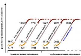
The origins of many of the technologies we still use today are believed to have occurred at the turn of the 18th and 19th centuries, when manual labor was replaced by heat engines, first in textiles and then in other industries. This sudden transition to machine production is usually called the industrial revolution. The Industrial Revolution led not only to the massive use of machines, but also to a change in the entire structure of society - there was a transformation of an agrarian society into an industrial one. As a result, labor productivity and people's living standards increased sharply.
The Industrial Revolution, which began in the textile industry, spurred the development of railway communication technologies. In turn, further growth in the transportation of various goods was impossible without new automotive technologies. Thus, every new technology always causes the birth and development of related technologies.

The Second World War contributed to the birth of new technologies - information, and therefore the period of time in which we live is called the information revolution (see figure). The beginning of the information revolution coincided with the development of computer technologies, without which the life of a modern person seems unthinkable.
The development of computer technology has always been associated with the miniaturization of electronic circuit elements. Currently, the size of one logical element (transistor) of a computer circuit is about 10-7 m, and scientists believe that further miniaturization of computer elements is possible only when special technologies called “NANOTECHNOLOGIES” are developed.
What is "nano"?
Translated from Greek, the word “nano” means dwarf. One nanometer (nm) is one billionth of a meter (10 -9 m). A nanometer is very, very small. A nanometer is the same number of times less than one meter as the thickness of a finger is less than the diameter of the Earth. Most atoms have a diameter of 0.1 to 0.2 nm, and the thickness of the DNA strands is about 2 nm. The diameter of red blood cells is 7000 nm, and the thickness of a human hair is 80,000 nm.

The figure shows a variety of objects from left to right in order of increasing size - from the atom to the solar system. Man has already learned to benefit from objects of various sizes. We can split the nuclei of atoms to produce atomic energy. By carrying out chemical reactions, we obtain new molecules and substances with unique properties. With the help of special tools, man has learned to create objects - from a pinhead to huge structures that are visible even from space.
However, if you look at the figure, you will notice that there is a fairly large range (on a logarithmic scale) where scientists have not set foot for a long time - between a hundred nanometers and 0.1 nm. Nanotechnology, which has been talked about so much lately, will have to work with objects ranging in size from 0.1 nm to 100 nm. And there is every reason to believe that we can make the nanoworld work for us.
Before our eyes, science fiction is becoming reality - it is becoming possible to move individual atoms and put them together, like cubes, into devices and mechanisms of unusually small sizes and therefore invisible to the ordinary eye. Nanotechnology, using the latest achievements of physics, chemistry and biology, is not just a quantitative, but a qualitative leap from working with matter to manipulating individual atoms.
Richard Feynman - prophet of the nanotechnology revolution
Airplanes, rockets, televisions and computers changed the world around us in the 20th century. Scientists argue that in the coming 21st century, the core of the new technical revolution will be materials, medicines, devices, communications and delivery means made using nanotechnology.
The idea that it might be possible to assemble devices and work with objects that are nanoscale was first proposed in a 1959 speech by Nobel laureate Richard Feynman at Caltech (“There's plenty of room down there!”). The word “below” in the title of the lecture meant in “a world of very small dimensions.” Then Feynman said that someday, for example, in 2000, people will wonder why scientists in the first half of the 19th century jumped through this nanoscale range of sizes, concentrating all their efforts on studying the atom and the atomic nucleus. According to Feynman, people lived for a very long time without noticing that a whole world of objects lived next to them, which were impossible to see. Well, if we didn’t see these objects, then we couldn’t work with them.
However, we ourselves consist of devices that have perfectly learned to work with nano-objects. These are our cells - the bricks that make up our body. The cell works with nanoobjects throughout its life, assembling molecules of complex substances from various atoms. Having collected these molecules, the cell places them in different parts - some end up in the nucleus, others in the cytoplasm, and others in the membrane. Imagine the possibilities that will open up for humanity if it masters the same nanotechnology that every human cell already possesses.
Feynman describes the consequences of the nanotechnology revolution for computers. “If, for example, the diameter of the connecting wires ranges from 10 to 100 atoms, then the size of any circuit will not exceed several thousand angstroms. Everyone who is associated with computer technology knows about the opportunities that its development and complication promises. If the number of elements used increases by millions of times, the capabilities of computers will expand significantly. They will learn to reason, analyze experience and calculate their own actions, find new computational methods, etc. An increase in the number of elements will lead to important qualitative changes in the characteristics of the computer.”
Having called scientists to the nanoworld, Feynman immediately warns about the obstacles that await them there, using the example of manufacturing a microcar only 1 mm long. Since the parts of an ordinary car are made with an accuracy of 10-5 m, the parts of a microcar should be made with an accuracy of 4000 times higher, i.e. 2.5.10-9 m. Thus, the dimensions of the microcar parts must correspond to the calculated ones with an accuracy of ± 10 layers of atoms.
The nanoworld is not only full of obstacles and problems. Good news awaits us in the nanoworld - all the parts of the nanoworld turn out to be very durable. This happens due to the fact that the mass of nanoobjects decreases in proportion to the third power of their size, and their cross-sectional area decreases in proportion to the second power. This means that the mechanical load on each element of the object - the ratio of the weight of the element to its cross-sectional area - decreases in proportion to the size of the object. Thus, a proportionally reduced nanotable has nanolegs that are a billion times thicker than necessary.
Feynman believed that a person could easily master the nanoworld if he created a robotic machine capable of making a smaller but workable copy of himself. Let, for example, we learn how to make a robot that can create a copy of itself reduced by 4 times without our participation. Then this little robot will be able to make a copy of the original one, reduced by 16 times, etc. It is obvious that the 10th generation of such robots will create robots whose dimensions will be millions of times smaller than the original ones

Of course, as we shrink in size, we will continually encounter very unusual physical phenomena. The insignificant weight of the nanorobot parts will lead to the fact that they will stick to each other under the influence of intermolecular interaction forces, and, for example, a nut will not be separated from a bolt after unscrewing. However, the laws of physics known to us do not prohibit creating objects “atom by atom.” Manipulation of atoms is, in principle, quite real and does not violate any laws of nature. The practical difficulties of its implementation are due only to the fact that we ourselves are too large and cumbersome objects, as a result of which it is difficult for us to carry out such manipulations.
To somehow stimulate the creation of micro-objects, Feynman promised to pay $1,000 to anyone who could build an electric motor measuring 1/64 inch (1 inch » 2.5 cm). And very soon such a micromotor was created. Since 1993, the Feynman Prize has been awarded annually for outstanding achievements in the field of nanotechnology.

In his lecture, Feynman also spoke about the prospects of nanochemistry. Chemists now use complex and varied techniques to synthesize new substances. Once physicists create devices that can manipulate individual atoms, many methods of traditional chemical synthesis can be replaced by “atomic assembly” techniques. At the same time, as Feynman believed, physicists, in principle, can really learn to synthesize any substance based on a written chemical formula. Chemists will order synthesis, and physicists will simply “arrange” atoms in the proposed order. The development of manipulation techniques at the atomic level will solve many problems in chemistry and biology.
Machines of creation by E. Drexler
Nanotechnology became a field of science in its own right and became a long-term technical project following detailed analysis by American scientist Eric Drexler in the early 1980s and the publication of his book Engines of Creation: The Coming Era of Nanotechnology.

This is how his book begins. “COAL and DIAMONDS, sand and computer chips, cancer and healthy tissue - throughout history, depending on the ordering of atoms, cheap or precious, sick or healthy arose. Arranged in the same way, the atoms make up soil, air and water; ordered by another, they constitute ripe strawberries. Arranged in one way, they form houses and fresh air; ordered by others, they form ash and smoke.
Our ability to arrange atoms is at the heart of technology. We have come far in our ability to arrange atoms, from sharpening flint for arrowheads to processing aluminum for spacecraft. We are proud of our technology, our life-saving medicines and desktop computers. However, our spaceships are still crude, our computers are still stupid, and the molecules in our tissues are still gradually disordered, first destroying health and then life itself. For all our success in ordering atoms, we still use primitive ordering methods. With our current technology, we are still forced to manipulate large, poorly controlled groups of atoms.
But the laws of nature provide many opportunities for progress, and the pressure of global competition always pushes us forward. For better or worse, the greatest technological advance in history lies ahead of us.”
According to Drexler's definition, nanotechnology is “an expected production technology focused on the low-cost production of devices and substances with a predetermined atomic structure.” Many experts believe that over the next 50 years, many devices will become so small that a thousand of these nanomachines could easily fit in the area occupied by the dot at the end of this sentence. To assemble nanomachines, you need:
- learn to work with single atoms - take them and put them in the right place.
- develop assemblers - nanodevices that could work with single atoms as explained in (1), using programs written by a person, but without his participation. Since each manipulation of an atom requires a certain amount of time, and there are a lot of atoms, scientists estimate that it is necessary to produce billions or even trillions of such nanoassemblers so that the assembly process does not take much time.
- develop replicators - devices that would be produced by nanoassemblers, because they will have to be made very, very many.
It will be years before nanoassemblers and replicators appear, but their appearance seems almost inevitable. Moreover, each step along this path will make the next one more real. The first steps towards creating nanomachines have already been taken. These are “genetic engineering” and “biotechnology”.
Heisenberg's Uncertainty Principle and Nanomachines
It is known from quantum physics that it is impossible to accurately determine the location of a particle and its momentum. Does this limit what nanomachines can do?
Indeed, the uncertainty principle makes the location of electrons quite vague, and this vagueness determines the size and structure of atoms. However, the atom as a whole has a relatively definite location, because the mass of its nucleus is thousands of times greater than that of electrons. Moreover, if atoms did not maintain their position relatively well, molecules would not exist. Therefore, the uncertainty principle does not impose significant restrictions on the accuracy with which atoms can be placed in their places when constructing nanomachines.
However, there is no need at all to use quantum mechanics to answer the question posed above. After all, the molecular machines existing in every living cell, which assemble “atom-by-atom” huge protein molecules of nanosize, already prove that nanomachines are possible!
Thermal vibrations of molecules and nanomachines
Analyzing the possibilities of creating nanomachines, E. Drexler discusses in his book how thermal vibrations of molecules can affect the operation of these machines. Will these fluctuations lead to numerous errors in the operation of nanomachines?
The molecular machines of living cells, which work perfectly at temperatures of about 300 K, despite the thermal vibrations of the molecules, again help to answer this question. Studies have shown that in some cells, when copying DNA, only ONE error is made per 100,000,000,000 operations! To achieve such high precision, living cells use special nanomachines, such as the enzyme DNA polymerase I, that check the copy and correct copying errors. It is clear that similar error checking and error correction algorithms will be needed for future automated nanomachinery assemblers.
Healing machines
E. Drexler proposed using nanomachines to treat humans. The human body is made of molecules, and people become sick and old because “unnecessary” molecules appear, and the concentration of “needed” ones decreases or their structure changes. As a result of this, people suffer. Nothing prevents a person from inventing nanomachines capable of rearranging atoms in “spoiled” molecules or reassembling them. It is obvious that such nanomachines can revolutionize medicine.
In the future, nanomachines (nanorobots) will be created, adapted to penetrate a living cell, analyze its condition and, if necessary, “treat” it by changing the structure of the molecules of which it consists. These nanomachines, designed to repair cells, would be comparable in size to bacteria and would move through human tissue the way leukocytes (white blood cells) do and enter cells like viruses do.
With the creation of nanomachines for cell repair, treating a patient will turn into a sequence of the following operations. First, working molecule by molecule and structure by structure, nanomachines will restore (heal) cell by cell of any tissue or organ. Then, working organ by organ throughout the body, they will restore the person's health.

Schematic representation of a nanorobot on the surface of a cell. The nanorobot's tentacles can be seen penetrating inside the cell. Author: Yu. Svidinenko. Taken from http://www.nanonewsnet.ru/
Photolithography – the road to the nanoworld: from top to bottom
Scientists and technologists have long been striving to enter the world of small sizes, especially those who develop new electronic devices and devices. For an electronic device to be smart and reliable, it must consist of a huge number of blocks, which means it must contain thousands and sometimes millions of transistors.
Optical photolithography is used in the manufacture of transistors and integrated circuits. Its essence is as follows. A layer of photoresist (a polymer light-sensitive material) is applied to the oxidized silicon surface, and then a photomask is applied to it - a glass plate with a pattern of integrated circuit elements

A beam of light passes through the photomask, and where there is no black color, the light hits the photoresist and illuminates it

After this, all those areas of the photoresist that were not treated with light are removed, and those that were illuminated are subjected to heat treatment and chemical etching. Thus, a pattern is formed on the surface of the silicon oxide, and the silicon wafer is ready to become the main part of the electronic circuit.
The transistor was invented in 1947, and then its dimensions were about 1 cm. Improvements in photolithographic methods made it possible to increase the size of the transistor to 100 nm. However, the basis of photolithography is geometric optics, which means that using this method it is impossible to draw two parallel straight lines at a distance less than the wavelength. Therefore, now photolithographic manufacturing of microcircuits uses ultraviolet light with a short wavelength, but further reducing the wavelength becomes expensive and difficult, although modern technologies already use electron beams to create microcircuits.
The introduction into the world of nanoscale dimensions, which chip manufacturers have followed until now, can be called a “top-down” road. They use technologies that have proven themselves in the macro world and are only trying to change the scale. But there is another way - “bottom up”. What if we force the atoms and molecules themselves to self-organize into ordered groups and structures several nanometers in size?
Examples of self-organization of molecules that form nanostructures are carbon nanotubes, quantum dots, nanowires and dendrimers
(Based on materials from Bogdanov K.Yu.)
Nanotechnologies are technologies that operate on quantities on the order of a nanometer.
The lines given here as an epigraph are taken from a fantasy work and cannot yet claim to be taken seriously by an ordinary person. But for a modern nanotechnology specialist, Lemov’s fantasies are no longer a utopia, but everyday work.
There is perhaps no exhaustive definition for the concept of nanotechnology, but by analogy with currently existing microtechnologies, it follows that nanotechnologies are technologies that operate with quantities on the order of a nanometer. This is a negligible value, hundreds of times shorter than the wavelength of visible light and comparable to the size of atoms. Therefore, the transition from “micro” to “nano” is no longer a quantitative, but a qualitative transition - a leap from the manipulation of matter to the manipulation of individual atoms.
When it comes to the development of nanotechnology, there are three directions in mind:
production of electronic circuits (including volumetric ones) with active elements with dimensions comparable to those of molecules and atoms;
development and production of nanomachines, i.e. mechanisms and robots the size of a molecule;
the direct manipulation of atoms and molecules and the assembly of everything that exists from them.
The implementation of all these areas has already begun. Almost ten years ago, the first results on moving single atoms and assembling certain structures from them were obtained, and the first nanoelectronic elements were developed and manufactured. According to experts, the production of nanoelectronic chips, for example, memory chips with a capacity of tens of gigabytes, will begin at the turn of the next century.
Nanotechnological control of products and materials, literally at the atomic level, has become commonplace in some areas of industry. A real example is DVDs, the production of which would be impossible without nanotechnological matrix control.
Existing methods of deposition of impurities in semiconductors (epitaxy) using lithographic templates have already practically approached their limit, not only in terms of size, but also topologically. The fact is that current photolithography technologies make it possible to produce only planar structures - when all elements and conductors are located in the same plane. And this imposes significant limitations on circuit design: the most advanced circuit solutions cannot be implemented using such technology.
In particular, it is impossible to reproduce the neural circuits on which great hopes are placed in this way. At the same time, nanotechnological methods are now being actively developed, making it possible to create active elements (transistors, diodes) the size of a molecule and form multilayer three-dimensional circuits from them. Apparently, microelectronics will be the first industry where “atomic assembly” will be carried out on an industrial scale.
Although we now have the means to manipulate individual atoms, they can hardly be used “directly” to assemble anything practically necessary, if only because of the number of atoms that would have to be “assembled.”
However, the capabilities of existing technologies are already sufficient to construct from several molecules some simple mechanisms that, guided by control signals from the outside (acoustic, electromagnetic, etc.), will be able to manipulate other molecules and create similar devices or more complex mechanisms.
They, in turn, will be able to manufacture even more complex devices, etc. Eventually, this exponential process will lead to the creation of molecular robots—machines comparable in size to large molecules and with their own built-in computer.
Prospects
Due to the introduction of logical nanoelements into all attributes of the environment, it will become “intelligent” and extremely comfortable for humans
MEDICINE
Creation of molecular robot doctors that would “live” inside the human body, eliminating all damage that occurs, or preventing the occurrence of such, including genetic damage. The projected implementation period is the first half of the 21st century.
GERONTOLOGY
Achieving personal immortality of people through the introduction of molecular robots into the body that prevent cell aging, as well as restructuring and “ennobling” the tissues of the human body. Revival and healing of those hopelessly ill people who were currently frozen by cryonics methods. Projected implementation period: third - fourth quarter of the 21st century.
INDUSTRY
Replacing traditional production methods with molecular robots assembling consumer goods directly from atoms and molecules. Up to personal synthesizers and copying devices that allow you to make any item. The first practical results can be obtained at the beginning of the 21st century.
AGRICULTURE
Replacement of “natural machines” for food production (plants and animals) with their artificial analogues - complexes of molecular robots. They will reproduce the same chemical processes that occur in a living organism, but in a shorter and more efficient way. For example, from the chain “soil - carbon dioxide - photosynthesis - grass - cow - milk” all unnecessary links will be removed. What will remain is “soil - carbon dioxide - milk (cottage cheese, butter, meat - whatever).” Needless to say, such “agriculture” will not depend on weather conditions and will not require hard physical labor. And its productivity is enough to solve the food problem once and for all. According to various estimates, the first such complexes will be created in the second to fourth quarters of the 21st century.
BIOLOGY
It will become possible to “introduce” into a living organism at the atomic level. The consequences can be very different - from the “restoration” of extinct species to the creation of new types of living beings, biorobots. Projected implementation period: mid-21st century.
ECOLOGY
Complete elimination of the harmful effects of human activities on the environment. Firstly, by saturating the ecosphere with molecular robotic nurses that transform human waste into raw materials, and secondly, by transferring industry and agriculture to waste-free nanotechnological methods. Projected implementation period: mid-21st century.
SPACE EXPLORATION
Apparently, space exploration in the “usual” order will be preceded by its exploration by nanorobots. A huge army of robotic molecules will be released into near-Earth space and prepare it for human settlement - make the Moon, asteroids, nearby planets habitable, and build space stations from “survival materials” (meteorites, comets). It will be much cheaper and safer than current methods.
CYBERNETICS
There will be a transition from currently existing planar structures to volumetric microcircuits, and the sizes of active elements will decrease to the size of molecules. The operating frequencies of computers will reach terahertz values. Circuit solutions based on neuron-like elements will become widespread. A high-speed long-term memory based on protein molecules will appear, the capacity of which will be measured in terabytes. It will become possible to “relocate” human intelligence into a computer. Projected implementation period: first - second quarter of the 21st century.
SMART HABITAT
By introducing logical nanoelements into all attributes of the environment, it will become “intelligent” and extremely comfortable for humans. Projected implementation period: after the 21st century.
Elements of information systems
This makes it possible to reduce the size of one transistor to approximately 10 nm, and increase operating frequencies to about 1012 Hz.
INTRODUCTION
Nanoelectronic elements developed in recent years, in their miniature size, speed and power consumption, seriously compete with traditional semiconductor transistors and integrated circuits based on them as the main elements of information systems.
Already today, technology has come close to the theoretical possibility of storing and transmitting 1 bit of information using one electron, the localization of which in space can be specified by one atom. This makes it possible to reduce the size of one transistor to approximately 10 nm, and increase operating frequencies to about 1012 Hz.
QUANTUM FUNDAMENTALS OF NANOELECTRONICS
When moving to the nanoscale, the quantum properties of the objects under consideration come to the fore. From the standpoint of quantum mechanics, an electron can be represented by a wave described by the corresponding wave function. The propagation of this wave in nanoscale solid structures is controlled by quantum confinement effects, interference, and the ability to tunnel through potential barriers.
A specific manifestation of quantum confinement is single-electron tunneling under Coulomb blockade conditions. Let us consider the example illustrated in the following figure of an electron passing through a metal-insulator-metal structure.
Initially, the interface between the dielectric and the metal is electrically neutral. When a potential is applied to metallic regions, charge begins to accumulate at this boundary. This continues until its magnitude is sufficient to separate and tunnel through the dielectric one electron. After the act of tunneling, the system returns to its original state. When the external applied voltage is maintained, everything repeats again. Thus, charge transfer in the structure is carried out in portions equal to the charge of one electron.
NANOELECTRONIC ELEMENTS
One of the first to appear were elements based on resonant tunneling, which were a double-barrier diode based on quantum wells, in which the well potential and the corresponding resonant conditions were controlled by a third electrode.
A tunnel transistor consists of two tunnel junctions connected in series. Tunneling of individual electrons is controlled by Coulomb blockade, controlled by a potential applied to the active region of the transistor in its middle between two layers of solid dielectric. If we imagine one bit as the presence or absence of one electron, then a 100 GB memory circuit would fit on a chip with an area of only 6 cm2.
In 1993, a new family of digital switching devices based on atomic and molecular cords was developed. On this basis, the logical elements NAND and NOR were developed. The size of such a structure is ~ 10 nm, and the operating frequency is ~ 10 12 Hz.
Quantum dots
GENERAL INFORMATION
Semiconductor quantum dots are on the order of a nanometer in size, giant molecules consisting of 103 - 105 atoms, created on the basis of conventional inorganic semiconductor materials Si, InP, CdSe, etc. They are larger than traditional molecular clusters typical for chemistry (~ 1 nm with a content of no more than 100 atoms), but smaller than nanometer-sized structures produced by modern lithographic means in the electronics industry.
The analogy with atomic physics (but with a compression of the energy scale by a factor of 10,000!) allows us to study “atom-like physics” using magnetic fields available in laboratory conditions.
QUANTUM DOTS CAN BE PRODUCED THROUGH
- colloidal chemicals
- controlled solidification during epitaxial growth
- size fluctuations in conventional quantum wells
- nanomanufacturing
COLLOIDAL POINTS
Colloidal points are free, i.e. they are not buried inside another semiconductor. Thus they are free from tension. They are covered with organic molecules used to prevent the little dots from curling up as they grow. The size of these molecules can be controlled during growth and their shape approaches spherical. Colloidal technologies have been developed quite deeply mainly for ionic systems II - IV (CdS, CdSe) and recently for group III - V semiconductors (InP, GaP, InAs). Due to the perfect versatility of dimensions, high-resolution spectroscopic studies can be carried out. The latter revealed new physical effects, including a significant expansion of electron-hole exchange interactions with respect to corresponding massive solids, excited state charge transfer, unusual (mass) behavior under pressure (e.g., delayed phase transitions), and the definition of up to 10 excited states electron-hole transitions. It is now possible to replace the organic etched shell around these points with inorganic semiconductors - for example: CdSe (ZnS) - thus producing core-shell structures. Arrays of colloidal dots were created. Moreover, input structures that prohibit the loading of colloidal quantum dots with carriers have recently become possible for dots measuring 6 nm.
CONTROLLED SOLIDIFICATION
Controlled solidification of a film of material A grown on a substrate created from material B produces islands A, since the difference between the atomic sizes of A and B is quite large. Examples of A/B pairs include InAs|GaAs and InP|GaInP. If organometallic chemical evaporation or molecular beam epitoxic growth is stopped immediately before island merging, a surprisingly versatile set of material A points can be obtained.
The shapes of these points vary greatly. They appear in the form of pyramids, but the accumulation changes the shape and composition. Usually only a small number of sizes can be obtained. Spectroscopic and transport changes at these points revealed multiexciton transitions (multiple electrons and multiple holes decaying together). Coulomb blockade effects have also been discovered, where loading a point with electrons causes Coulomb repulsion of electrons from other electrons so electron addition requires an increased input voltage. Vertical alignment of self-assembled dots currently holds promise for point mesh generation and device applications.
SIZE FLUCTUATIONS IN QUANTUM WELLS
Size fluctuations in quantum wells disrupt the periodicity in the two extended directions, thus causing the formation of a dot. Controlling shape and size is quite complex, but the quality of susceptibility is so good that extremely precise spectroscopic features can be observed. In fact, many of the recent advances in single-point spectroscopy and nanonuclear magnetic resonance or nanophotolumenescence have focused on this type of point.
NANOPRODUCTION
Nanofabrication of quantum dots is ideal for studying transport properties such as observing the transition of electrons individually into dots. This reveals a beautiful sequence of transitions, re-arranging atomic physics in its selection rule, but on the energy scale of millielectronvolts (instead of about 10eV). The analogy with atomic physics (but with a compression of the energy scale by a factor of 10,000!) allows us to study “atom-like physics” using magnetic fields available in laboratory conditions.
Quantum dots make it possible to study ordinary quantum structures that you can read about in a textbook, in laboratory conditions (for example, “particle in a box”) at the maximum limit of the zero dimension (i.e., no periodicity), and to study unusual behavior that can be new concepts for various devices are based. Among the latter are highly economical quantum lasers, light-emitting diodes, solar cells and single-electron transistors. Thus, this area is of interest to theorists of quantum physics, experimenters in the field of electroscopy, information transmission, and, probably, specialists in the field of optoelectronics. In fact, today it is difficult to find a conference in physics, chemistry or materials science where one of the key issues is not the question of quantum dots.
1. Definitions and terminology
2. Nanotechnology: history of origin and development
3. Fundamentals
Scanning probe microscopy
Nanomaterials
Nanoparticles
Self-organization of nanoparticles
The problem of agglomerate formation
Micro- and nanocapsules
Nanotechnology sensors and analyzers
4. Applications nanotechnology
Medicine and biology
In the automotive industry
Agriculture
Ecology
Space exploration
Cybernetics
5. Society's attitude towards nanotechnology
Nanotechnology is an interdisciplinary field of fundamental and applied science and technology, dealing with a set of theoretical justification, practical methods of research, analysis and synthesis, as well as methods for the production and use of products with a given atomic structure through the controlled manipulation of individual atoms and molecules.
Nanotechnology is a technology for studying nanometer-scale objects, and working with objects on the order of a nanometer (a millionth of a millimeter), which is comparable to the size of individual molecules and atoms.
Definitions and terminology
In Technical Committee ISO/TC 229, nanotechnology means the following:
knowledge and control of processes, typically at the 1 nm scale, but not excluding the sub-100 nm scale, in one or more dimensions, where the introduction of a size effect (phenomenon) leads to the possibility of new applications;
the use of properties of objects and materials on a nanometer scale, which differ from the properties of free atoms or molecules, as well as from the bulk properties of a substance consisting of these atoms or molecules, to create more advanced materials, devices, systems that realize these properties.
According to the “Development Concept in Russia works in the field of nanotechnology until 2010" (2004) nanotechnology is defined as a set of methods and techniques that provide the ability to create and modify objects in a controlled manner, including components with dimensions less than 100 nm, at least in one dimension, and as a result of this, obtaining fundamentally new qualities that allow their integration into fully functioning systems of a larger scale.


The practical aspect of nanotechnology involves the production of devices and their components needed to create, process and manipulate atoms, molecules and nanoparticles. It is understood that an object does not necessarily have to have at least one linear size less than 100 nm - these can be macro-objects, the atomic structure of which is controlled in a controlled manner with resolution at the level of individual atoms, or they can contain nano-objects. In a broader sense, this term also covers methods of diagnosis, characterology and research of such objects.
Nanotechnologies are qualitatively different from traditional disciplines, since on such scales the usual, macroscopic technologies for handling matter are often inapplicable, and microscopic phenomena, negligibly weak on conventional scales, become much more significant: the properties and interactions of individual atoms and molecules or aggregates of molecules (for example, Van forces -der Waals), quantum effects.


Nanotechnology and especially molecular technology are new, very little explored disciplines. The major discoveries predicted in this area have not yet been made. However, ongoing research is already yielding practical results. The use of advanced scientific achievements in nanotechnology allows us to classify it as high technology.


The development of modern electronics is moving along the path of reducing the size of devices. On the other hand, classical production methods approach their natural economic and technological barrier, when the size of the device does not decrease much, but the economic ones increase exponentially. Nanotechnology is the next logical step in the development of electronics and other high-tech industries.
Nanotechnology is a logical continuation and development of microtechnology.

Microtechnology, a combination of science that studies micro-objects and technology work with objects on the order of a micrometer (a thousandth of a millimeter), became the basis for the creation of modern microelectronics. Cell phones, computers, the Internet, a variety of household, industrial and consumer electronics, all this has changed both the world and people beyond recognition.

Nanotechnology will change the world just as much. Nanotechnology requires very large computing power to simulate the behavior of atoms, and high-precision electrical and mechanical devices to arrange the atoms and molecules of different materials in new ways. In this way new matter is created. For the first time in the history of civilization, materials with new properties that people need are being created. Let's list just a few of them. This is a transparent and flexible material with the lightness of plastic and the hardness of steel, a flexible plastic coating that is a solar battery, a material for the electrode of an electric battery, which is tens and hundreds of times stronger than a regular one.

Even at the modern level, nanotechnology makes it possible to obtain flexible plastic screens with the thickness of a paper sheet and the brightness of a modern monitor, compact electronics based on carbon compounds, with dimensions and energy intensity hundreds of times lower than modern ones. Nanotechnology also means lightweight and flexible structural and building materials, highly efficient filters for air and water, medicines and cosmetics that act on a deeper level, a rapid reduction in the cost of space flight, and much, much more.

So far, all nanotechnological materials are very expensive. But, as with the computer industry, mass production will lead to dramatic price compromises. In the invisible struggle for the profits and influence that nanotechnology will give, the main speculators are the United States, and Russia. Israel, European countries, and countries Latin America is rapidly increasing its potential in this area.

Unfortunately, despite the presence of a good scientific base and large private capital, Ukrainian scientific developments and applied products are poorly represented in the world.
Scientific national nanotechnology programs are of particular importance for nanotechnological developments. More than 50 developed countries announced the launch of their own nanotechnology programs.
Nanotechnology: history of origin and development
Many sources, primarily English-language ones, associate the first mention of methods that would later be called nanotechnology with Richard Feynman’s famous speech “There’s Plenty of Room at the Bottom,” made by him in 1959 in California Institute of Technology at the annual meeting of the American Physical Society.

Richard Feynman suggested that it might be possible to mechanically move single atoms using a manipulator of the appropriate size, at least this size process would not contradict currently known physical laws.

He suggested doing this manipulator in the following way. It is necessary to build a mechanism that would create a copy of itself, only an order of magnitude smaller. The created smaller mechanism must again create a copy of itself, again an order of magnitude smaller, and so on until the dimensions of the mechanism are commensurate with the dimensions of the order of one atom. In this case, it will be necessary to make changes in the structure of this mechanism, since the gravitational forces acting in the macrocosm will have less and less influence, and the forces of intermolecular interactions and van der Waals forces will increasingly influence the operation of the mechanism. The last stage - the resulting mechanism will assemble its copy from individual atoms. In principle, the number of such copies is unlimited; it will be possible to create an arbitrary number of such machines in a short time. These machines will be able to assemble macro-things in the same way, by atomic assembly. This will make things much cheaper - such robots (nanorobots) will need to be given only the required number of molecules and energy, and write a program to assemble the necessary items. So far, no one has been able to refute this possibility, but no one has yet managed to create such mechanisms. This is how R. Feynman described his alleged manipulator:
I'm thinking about creating an electrically controlled system that uses conventionally manufactured "service robots" in the form of four-times smaller copies of the operator's "hands." Such micro-mechanisms will be able to easily perform operations on a reduced scale. I'm talking about tiny robots equipped with servo motors and small "arms" that can tighten equally small bolts and nuts, drill very small holes, etc. In short, they will be able to do all the work at 1:4 scale. To do this, of course, the necessary mechanisms, tools and manipulating arms must first be made to one-fourth the usual size (in fact, it is clear that this means reducing all contact surfaces by a factor of 16). In the final stage, these devices will be equipped with servo motors (with 16 times reduced power) and connected to a conventional electrical control system. After this, you will be able to use manipulator arms that are 16 times smaller! The scope of application of such microrobots, as well as micromachines, can be quite wide - from surgical operations to the transportation and processing of radioactive materials. I hope that the principle of the proposed program, as well as the unexpected problems and exciting opportunities associated with it, are clear. Moreover, you can think about the possibility of a further significant reduction in scale, which, naturally, will require further design changes and modifications (by the way, at a certain stage, you may have to abandon the “hands” of the usual shape), but will make it possible to produce new, much more advanced devices of the described type. Nothing stops me from continuing this process and create as many tiny machines as you want, since there are no restrictions related to the placement of machines or their material consumption. Their volume will always be much less than the volume of the prototype. It is easy to calculate that the total volume of 1 million machines reduced by 4000 times (and therefore the mass of materials used for manufacturing) will be less than 2% of the volume and weight of a conventional machine of normal dimensions.
It is clear that this immediately removes the problem cost materials. In principle, it would be possible to organize millions of identical miniature factories, in which tiny machines would continuously drill holes, stamp parts, etc. As we get smaller, we will constantly encounter very unusual physical phenomena. Everything you encounter in life depends on large-scale factors. In addition, there is also the problem of “sticking together” of materials under the influence of intermolecular interaction forces (the so-called van der Waals forces), which can lead to effects that are unusual on a macroscopic scale. For example, a nut will not separate from a bolt once unscrewed, and in some cases will "stick" tightly to the surface, etc. There are several physical problems of this type that should be kept in mind when designing and building microscopic mechanisms.

During the theoretical study of this possibility, hypothetical doomsday scenarios emerged, which assume that nanorobots will absorb all the biomass of the Earth, carrying out their self-reproduction program (the so-called “gray goo” or “gray slurry”).
The first assumptions about the possibility of studying objects at the atomic level can be found in the book “Opticks” by Isaac Newton, published in 1704. In the book, Newton expresses hope that future microscopes will one day be able to explore the “secrets of corpuscles.”

The term “nanotechnology” was first used by Norio Taniguchi in 1974. He used this term to describe the production of commercial items of size on the order of nanometers. In the 1980s, Eric K. Drexler used the term, most notably in his 1986 book Engines of Creation: The Coming Era of Nanotechnology. He used this term to refer to a new area of science that he was exploring in his doctoral dissertation at the Massachusetts Institute of Technology (MIT). He subsequently published the results of his research in the book Nanosystems: Molecular Machinery, Manufacturing, and Computation. Mathematical calculations played a major role in his research, since with their help it is still possible to analyze hypothetical properties and develop devices with dimensions on the order of nanometers.

Basically, the possibility of mechanical manipulation of molecules and the creation of self-replicating manipulators for these purposes are currently being considered.
As has already been said, this will make it possible to reduce the cost of any existing products many times over and create fundamentally new ones, solving all existing environmental problems. Also, such manipulators have enormous medical potential: they are capable of repairing damaged human cells, which actually leads to real technical immortality of a person. On the other hand, the creation of nanomanipulators may lead to the “gray sludge” scenario. They also suggest a possible scenario when a certain group of people gains complete control over such a manipulator and uses it to completely assert their position over other people. If this scenario comes true, the result will be an ideal one, which, apparently, will be impossible to destroy.
The most complete definition of NT is given in the materials of the national nanotechnology initiative USA:
NT - scientific research and technological developments at the atomic, molecular or macromolecular levels with a subnanometer scale along one or more coordinates to provide a fundamental understanding of the phenomena and properties of materials at such dimensions and for the manufacture and use of structures, devices and systems that have new properties and functions due to their small size.

At the same time, the work shows that the foundations of NT were laid in the second half of the 19th century in connection with the development of colloidal chemistry. In 1857, M. Faraday was the first to obtain stable colloidal solutions (sols) of gold that were red in color. In 1861, T. Graham managed to coagulate sols and turn them into gels. He also introduced the division of substances according to the degree of dispersion of the structure into colloidal (amorphous) and crystalloid (crystalline).
The crystalline or amorphous state of a substance depends, first of all, on its own properties, and then on the conditions under which the transition to the solid state occurs.

In 1869, the chemist I. Borshchov hypothesized that, depending on the conditions, a substance could be obtained in both a crystalline (tendency to form crystals) and a colloidal (amorphous) state. By appropriately changing the conditions for the transition of a substance into a solid state, it is possible to obtain typically amorphous substances (rubber, glue, glass) in a crystalline state and, conversely, to obtain typically crystalline substances (metals and table salt) in an amorphous (glassy) state.
Since in the 19th century there were only optical microscopes for observing objects and measuring their sizes, which did not allow detecting particles in colloidal solutions and grains in colloidal substances, substances with an ultra-high degree of dispersion, particles, fibers, grains and films of which cannot be detected in optical microscopes having a resolution of 300 nm when using white light and 150 nm when using ultraviolet light.
In 1892, D. Ivanovsky discovered the first biological colloidal particle, the tobacco mosaic disease virus, and in 1901, W. Reed isolated the first human virus, the yellow fever virus. It should be noted that viruses have characteristic sizes from 40 to 80 nm.

In 1903, R. Zsigmondy and R. Siedentopf invented an optical ultramicroscope, which had a resolution of up to 5 nm and made it possible to observe colloidal particles. An ultramicroscope is built on the principle of observation in reflected light, due to which smaller objects become visible than in an ordinary microscope. With the help of R. Zsigmondy’s ultramicroscope, it was possible to establish that in colloidal solutions (sols) gold yellow particles have a size of 20 nm, red - 40 nm, and blue - 100 nm.
In 1904, P. Weymarn established: Between the world of molecules and microscopically visible particles, there is a special form of matter with a complex of new physicochemical properties inherent in it - an ultradisperse or colloidal state, formed when its degree of dispersion is in the region of 105-107 cm-1, in in which the films have a thickness, and the fibers and particles have a diameter in the range of 1.0-100 nm.
The classification of the state of a substance according to the degree of dispersion is given in Table 1. It can be seen that the colloidal state is an extremely highly dispersed or ultradisperse state of a substance.
All dispersed systems are heterogeneous, since they consist of a continuous continuous phase - the dispersion medium and crushed particles located in it - the dispersed phase. A prerequisite for their existence is the mutual insolubility of the dispersed phase and the dispersion medium.

Colloidal systems are often called ultramicroheterogeneous to emphasize that phase separation in them cannot be detected using optical microscopes. If the particles of the dispersed phase have the same sizes, the systems are called monodisperse, and if they are different, then they are called polydisperse systems.
The properties of substances and materials depend on their structure, characterized by interconnected levels that influence such properties.
The first level of structure is called crystalline and characterizes the spatial arrangement of atoms, ions and molecules in the crystal lattice of a solid, which can be influenced by point defects (vacancies, atoms in interstices, foreign atoms). Point defects are mobile and largely determine the diffusion and electrical properties of materials, especially semiconductors.
The second level is associated with the presence in a solid of various linear and planar structural defects (dislocations), the number of which per unit volume increases under mechanical loads, leading to the appearance of internal stresses in the material. Like point defects, dislocations are mobile, and their density and ability to move in a solid determine the mechanical properties of materials, especially metals.
The third level of structure is volumetric defects such as pores and capillaries, which can be created in materials during their formation or use. They are associated with the absence of certain areas of the solid body.
All substances in the solid state can be divided into monocrystalline, polycrystalline, amorphous (or nanocrystalline) and molecular solid solutions.

If the ordered arrangement of particles (atoms, molecules or ions), reflected by the unit cell, is maintained throughout the entire volume of the solid, then single crystals are formed.
If the ordering of the structure is maintained in macroscopic (>100 µm) and microscopic (>0.1 µm) areas of the solid (see Table 1), then polycrystalline substances are formed with so-called crystallites or crystallite grains of appropriate sizes and spatially misoriented relative to each other crystal lattices.
Until the mid-1980s, it was believed that amorphous substances lack an ordered arrangement of particles. However, studies carried out using high-resolution electron transmission, scanning tunneling and atomic force microscopes, especially on metal glasses, made it possible to detect crystallites or grains with sizes in the subnanometer range in amorphous substances.

Thus, amorphous substances and materials are characterized by an ultradisperse (colloidal) degree of fragmentation of the grains of the crystalline phase, and they can be called nanocrystalline.
In molecular solid solutions, as in liquid solutions, usually called true solutions or simply solutions, the distributed substance is uniformly mixed with the molecules of the dispersion medium at the molecular level. Therefore, molecular solid and liquid solutions that do not have phases or interfaces are homogeneous systems.
The crystalline state of a substance is always more stable than the amorphous (nanocrystalline) state, therefore a spontaneous transition from the amorphous to the crystalline state is possible, but the reverse is not. An example is devitrification - the spontaneous crystallization of glass at elevated temperatures.
Dispersed systems, including colloidal ones, are classified according to the degree of dispersion, the state of aggregation of the dispersed phase and the dispersion medium, the intensity of interaction between them, the absence or formation of structures.
The diversity of colloidal systems is due to the fact that the phases that form them can be in any of three states of aggregation; have inorganic, organic and biological nature. Depending on the state of aggregation of the dispersed phase and the dispersion medium, the following 9 types of dispersed systems are possible:
Zh1 - G2, Zh1 - Zh2, Zh1 - T2,
T1 - G2, T1 - G2, T1 - T2,
G1 - G2, G1 - T2, T1(F1) - T1(F2),
where G, F and T are gaseous, liquid and solid states, and numbers 1 and 2 refer to the dispersed phase and dispersion medium, respectively. For the latter type of disperse system, F1 and F2 denote different phases (polymorphic modifications) of the solid state of one substance.
In a gaseous dispersion medium, only liquids and solids can be dispersed, since all gases dissolve indefinitely in each other at not very high pressures.
Dispersed systems with a gaseous dispersion medium are called aerosols. Fogs are aerosols with a liquid dispersed phase (L1 - G2), and smokes are aerosols with a solid dispersed phase (T1 - G2). The simplest example of an aerosol is tobacco smoke, the average particle size of which is 250 nm, while the particle size of soot or volcanic ash can be less than 100 nm, and their aerosols belong to ultrafine (colloidal) systems.
Gases, liquids and solids can be dispersed in a liquid dispersion medium. Foams are a dispersion of gas in liquid (G1 - G2). Emulsions are dispersed systems in which one liquid is crushed into another liquid that does not dissolve it (L1 - L2). Of greatest importance for chemistry and biology are colloidal systems in which the dispersion medium is the liquid phase, and the dispersed phase is a solid (T1 - L2), called colloidal solutions or sols, often lyosols. If the dispersion medium is water, then such sols are called hydrosols, and if an organic liquid, then they are called organosols. Colloidal solutions are very important, since many processes occurring in living organisms are associated with them.
Gases, liquids and solids can be dispersed in a solid dispersion medium. Systems (G1 - T2) are called solid foams or capillary dispersed systems, in which the gas is in the form of separate closed cells separated by a solid dispersion medium. Solid foams include polystyrene foam, foam concrete, pumice, slag, metals with the inclusion of gases, various porous materials (activated carbon, silica gel, wood), as well as membranes and diaphragms, photonic crystal fibers, leather, paper, fabrics.

The system (G1 - T2) includes a wide class of crystalline hydrates - crystals containing molecules of water of crystallization. Typical crystalline hydrates are many natural minerals, for example, gypsum CaSO4∙2H2O, carnallite MgCl2∙KCl∙6H2O, potassium alum KAl(SO4)2·12H2O.
Dispersed systems of type (T1 - T2) are of great practical importance, which include the most important building materials, metal-ceramic compositions, some alloys, enamels, a number of minerals, in particular some precious and semi-precious stones, many rocks in which crystals were released when the magma solidified .
Colored glasses are formed as a result of the dispersion of metal nanoparticles or their oxides in silicate glass. Enamels are silicate glasses with inclusions of SnO2, TiO2 and ZrO2 pigments, which give the enamels opacity and color.
Thus, colloids are not understood as a separate class of substances, but as a special state of any substance, characterized, first of all, by certain particle sizes. Nanostructuring of a solid should be understood as the transfer of a substance or material into a colloidal (ultradisperse) state, i.e. the creation in the structure of physical or chemical phases of subnanometer sizes, which can be considered as peculiar nanoparticles separated from the rest of the structure by interfaces.
Such nanoparticles, in addition to mechanically dispersed nanopowders, are:
Nanocrystalline grains;
Nano-sized polymorphic phases;
Nano-sized structural defects (nanoblocks);
Surface nanostructures (pits, protrusions, grooves, walls);
Volumetric nanostructures (pores and capillaries);
Nano-sized chemical phases of foreign atoms or molecules, formed on its surface or in the volume and having a fibrous or corpuscular shape;
Nano-sized structures formed as a result of physical or chemical deposition from the gas or liquid phase (fullerenes, carbon nanotubes);
Films of nanosized substances formed in a periodic sequence;
Macromolecules, polymolecular assemblies, molecular films, molecular complexes of the “host-guest” type (the presence of a size distribution is a feature that distinguishes nanoparticles from macromolecules); nano-sized and nanostructured biological structures (viruses, proteins, genes, proteins, chromosomes, DNA and RNA molecules).
The colloidal state of a substance is a qualitatively special form of its existence with a complex of inherent physicochemical properties. For this reason, the field of natural science that studies the objective physical and chemical laws of the heterogeneous ultradisperse state of matter, high-molecular compounds ( polymers, complex compounds and molecular assemblies) and interphase surfaces, formed at the beginning of the twentieth century into an independent discipline - colloidal chemistry.
The rapid development of colloidal chemistry is due to the great importance of the phenomena and processes studied by this science in various areas of human practice. Such seemingly completely different areas as life processes in organisms, the formation of many minerals, the structure and productivity of soils are closely related to the colloidal state of matter. Colloidal chemistry is also the scientific basis for industrial production indices of many materials.
With the development of technical means for the formation and manipulation of nanoobjects, as well as methods for their study, more specialized disciplines began to emerge in colloid chemistry, such as chemistry polymers and surface physical chemistry (late 1950s), supramolecular chemistry (late 1970s).
The study and study of nanosized and nanostructured biological structures (proteins, genes, chromosomes, proteins, amino acids, DNA, RNA), which are the subject of the biology of ultradisperse systems, led to the creation of virology in the 30-50s, molecular biology and in the last quarter of the twentieth century genetics and immunochemistry.
If the dimensions of a material in at least one dimension are less than the critical lengths that characterize many physical phenomena, such a material acquires new unique physical and chemical properties of a quantum mechanical nature, which are studied and used to create new devices by the physics of low-dimensional structures, which is the most dynamically developing area of modern solid state physics bodies.
The result of studies of low-dimensional systems (quantum wells, wires and dots) was the discovery of fundamentally new phenomena - the integer and fractional quantum Hall effect in a two-dimensional electron gas, Wigner crystallization of quasi-two-dimensional electrons and holes, the discovery of new composite quasiparticles and electronic excitations with fractional charges.
The field of colloid chemistry, which studies the processes of deformation, destruction and formation of materials and dispersed structures, has evolved into the physical and chemical mechanics of solids and ultradisperse structures. It was formed in the mid-twentieth century thanks to the work of academician P. Rebinder and his school as new knowledge, borderline colloidal chemistry, molecular physics of solids, mechanics of materials and their production technology.
The main task of physical and chemical mechanics is the creation of structural materials with specified properties and an optimal structure for the purposes of their application.
Another branch that studies and creates elements, structures and devices in the subnanometer range is microelectronics, in which nanoelectronics can be distinguished (development and production of integrated circuits with subnanometer sized elements - integrated nanocircuits (INS), molecular electronics, functional electronics of nanostructured materials and nanoelectromechanical systems (NEMS).
Summarizing the above, as well as based on the analysis carried out in the work, we can formulate a definition of NT: nanotechnology is the controlled production of substances and materials in a colloidal (ultradisperse, nanostructured with the size of structural elements in the range of 1.0-100 nm) state, research and measurement their properties and characteristics and their use in various industries science, technology and industry.
All terms associated with the creation and study of the colloidal (nanostructured) level of the structure of matter under the brand “nanotechnology” automatically received the prefix “nano”, although until the mid-1980s they were called accordingly: mechanics, photonics, crystallography, chemistry, biology and electronics ultrafine or colloidal systems; and the objects of their research were named: ultrafine powders and composites, aero-, hydro- and organosols, reversible and irreversible gels, ultrafine ceramics, etc.
The emergence of interest in the colloidal state of matter under the brand “nanotechnology” in the last 20 years is due, firstly, to its unique properties, and secondly, to the development and creation of technological and control equipment for obtaining and studying the sub-nanoscale level of the structure of matter: its physics , chemistry and biology.
Instead of discovering new materials and phenomena through serendipity or chaotic research, the controlled transformation of matter into a nanostructured (colloidal) state, called the concept of nanotechnology, allows this to be done systematically. Instead of finding nanoparticles and nanostructures with good properties using intuition, knowledge of the laws of formation and stabilization of ultradisperse systems opens up the possibility of their artificial design according to a specific system.
Particularly interesting was the acquisition of completely new properties by some well-known substances at nanoscale sizes.
Nanostructured (colloidal) systems, in accordance with their intermediate position between the world of atoms and molecules and the world of microscopic and macroscopic bodies, can be obtained in two main ways: dispersion, i.e. grinding (crushing) of large systems, and condensation, i.e. the formation of nanosystems from atoms, molecules, clusters and nanostructures.
Methods for obtaining nanostructured systems using the first route are called dispersion, and the second – condensation. There are mixed methods for producing nanostructured systems, which are called dispersion-condensation and condensation-dispersion, respectively.
In traditional nanoelectronics, during the manufacture of integrated nanocircuits (ANCs) using classical CMOS technology, controlled nanostructuring of functional layers (FL) on silicon wafers is provided by projection (photo templates and nanostamps) mask (resistive masks) lithographic patterning.
In this case, a strategic dispersion approach or a top-down approach is used, i.e. Local removal of unnecessary areas of the FS is carried out by etching them. The accuracy of reproducing the dimensions of structural elements in the horizontal plane is ensured using resistive masks formed in lithography processes.
In this regard, emphasizing the strategic dispersion or top-down approach used, traditional industrial nanoelectronics is more conveniently called D-nanoelectronics.
Condensation methods (non-lithographic synthesis methods), which use a bottom-up approach to obtain nanostructured systems, can be divided into two groups: traditional and new, created within the framework of the latest advances in nanotechnology.
Fundamental provisions
Scanning probe microscopy
One of the methods used to study nanoobjects is scanning probe microscopy. Within the framework of scanning probe microscopy, both non-optical and optical techniques are implemented.
Studies of surface properties using a scanning probe microscope (SPM) are carried out in air at atmospheric pressure, vacuum and even in liquid. Various SPM techniques make it possible to study both conducting and non-conducting objects. In addition, SPM supports combination with other research methods, such as classical optical microscopy and spectral methods.
Using a scanning probe microscope (SPM), you can not only see individual atoms, but also selectively influence them, in particular, move atoms along the surface. Scientists have already managed to create two-dimensional nanostructures on the surface using this method. For example, at the IBM research center, by sequentially moving xenon atoms on the surface of a nickel single crystal, employees were able to lay out three letters of the logo companies using 35 xenon atoms.

When performing such manipulations, a number of technical difficulties arise. In particular, it is necessary to create ultra-high vacuum conditions (10−11 torr), it is necessary to cool the substrate and microscope to ultra-low temperatures (4-10 K), the surface of the substrate must be atomically clean and atomically smooth, for which special methods of its preparation are used. The substrate is cooled in order to reduce the surface diffusion of deposited atoms.
Nanomaterials
Nanomaterials are materials structured at or near the molecular size level. The structure may be more or less regular or random. Surfaces with a random nanostructure can be obtained by processing with particle beams, plasma etching and some other methods.

As for regular structures, small areas of the surface can be structured “from the outside” - for example, using a scanning probe microscope (see below). However, sufficiently large (~1 μ2 or more) areas, as well as volumes of matter, can be structured, apparently, only by the method of self-assembly of molecules.
Self-assembly is widespread in living nature. The structure of all tissues is determined by their self-assembly from cells; The structure of cell membranes and organelles is determined by self-assembly from individual molecules.
Self-assembly of molecular components is being developed as a way to construct periodic structures for fabricating nanoelectronic circuits, and notable advances have been made.
In medicine, materials with a nanostructured surface can be used to replace certain tissues. The cells of the body recognize such materials as “their own” and attach to their surface.

Currently, progress has been made in the production of nanomaterials that imitate natural bone tissue. Thus, scientists from Northwestern University ( USA) Jeffrey D. Hartgerink, Samuel I. Stupp and others used three-dimensional self-assembly of fibers about 8 nm in diameter, mimicking natural collagen fibers, followed by mineralization and formation of hydroxyapatite nanocrystals oriented along the fibers. Own bone cells were well attached to the resulting material, which allows it to be used as “glue” or “putty” for bone tissue.

It is also of interest to develop materials that have the opposite property: they do not allow cells to attach to the surface. One possible application of such materials could be the manufacture of bioreactors for growing stem cells. The fact is that, having attached to the surface, the stem cell strives to differentiate, forming certain specialized cells. The use of materials with nanoscale surface structure to control the processes of proliferation and differentiation of stem cells represents a huge field for research.

Nanopore membranes can be used in microcapsules for drug delivery and other purposes. Thus, they can be used to filter body fluids from harmful substances and viruses. Membranes can protect nanosensors and other implantable devices from albumin and similar coating substances.
Nanoparticles
The modern trend towards miniaturization has shown that a substance can have completely new properties if you take a very small particle of this substance. Particles ranging in size from 1 to 100 nanometers are commonly called “nanoparticles.” For example, it turned out that nanoparticles of some materials have very good catalytic and adsorption properties. Other materials show amazing optical properties, for example, ultra-thin films of organic materials are used to make solar cells. Such batteries, although they have a relatively low quantum efficiency, are cheaper and can be mechanically flexible. It is possible to achieve the interaction of artificial nanoparticles with natural nano-sized objects - proteins, nucleic acids, etc. Carefully purified nanoparticles can self-assemble into certain structures. This structure contains strictly ordered nanoparticles and also often exhibits unusual properties.

Nanoobjects are divided into 3 main classes: three-dimensional particles obtained by explosion of conductors, plasma synthesis, reduction of thin films, etc.; two-dimensional objects - films produced by molecular deposition, CVD, ALD, ion deposition, etc.; one-dimensional objects - whiskers, these objects are obtained by the method of molecular layering, introducing substances into cylindrical micropores, etc. There are also nanocomposites - materials obtained by introducing nanoparticles into any matrices. At the moment, only the microlithography method has been widely used, making it possible to obtain flat island objects with a size of 50 nm on the surface of matrices; it is used in electronics; The CVD and ALD method is mainly used to create micron films. Other methods are mainly used for scientific purposes. Particularly noteworthy are the ionic and molecular layering methods, since with their help it is possible to create real monolayers.
American organization C-Sixty Inc. Conducts preclinical tests of products based on C60 fullerene nanospheres with chemical groups ordered on their surface. These groups can be selected to bind to preselected biological targets. The range of possible applications is extremely wide. It includes the fight against viral diseases such as influenza and HIV, cancer and neurodegenerative diseases, osteoporosis, and vascular diseases. For example, a nanosphere may contain an atom of a radioactive element inside, and on the surface - groups that allow it to attach to a cancer cell.

Similar developments are being carried out in Russian Federation. The Institute of Experimental Medicine (St. Petersburg) used a fullerene adduct with polyvinylpyrrolidone (PVP). This compound is highly soluble in water, and the cavities in its structure are similar in size to C60 molecules. The cavities are easily filled with fullerene molecules, resulting in the formation of a water-soluble adduct with high antiviral activity. Since PVP itself does not have an antiviral effect, all activity is attributed to the C60 molecules contained in the adduct.
In terms of fullerene, its effective dose is approximately 5 μg/ml, which is significantly lower than the corresponding figure for rimantadine (25 μg/ml), traditionally used in the fight against the influenza virus. Unlike rimantadine, which is most effective in early period infection, the C60/PVP adduct has a stable effect throughout the entire virus reproduction cycle. Another distinctive feature of the constructed drug is its effectiveness against influenza viruses of type A and B, while rimantadine acts only on the first type.
Nanospheres can also be used in diagnostics, for example, as an X-ray contrast agent that attaches to the surface of certain cells and shows their location in the body.
Dendrimers are of particular interest. They represent a new type of polymers that have a branching structure rather than the usual linear one.
As a matter of fact, the first compound with such a structure was obtained back in the 50s, and the main methods for their synthesis were developed mainly in the 80s. The term “dendrimers” appeared earlier than “nanotechnology”, and at first they were not associated with each other. However, recently dendrimers are increasingly mentioned in the context of their nanotechnological (and nanomedicine) applications.

This is due to a number of special properties that dendrimer compounds have. Among them:
Predictable, controllable and reproducible sizes of macromolecules with great accuracy;
The presence of channels and pores in macromolecules that have well-reproducible shapes and sizes;
The ability for highly selective encapsulation and immobilization of low molecular weight substances with the formation of supramolecular “guest-host” constructs.
Self-organization of nanoparticles
One of the most important questions facing nanotechnology is how to force molecules to group in a certain way, to self-organize, in order to ultimately obtain new materials or devices. This problem is dealt with by a branch of chemistry—supramolecular chemistry. It studies not individual molecules, but interactions between molecules that are capable of ordering molecules in a certain way, creating new substances and materials. It is encouraging that similar systems and similar processes actually exist in nature. Thus, biopolymers are known that can organize into special structures. One example is proteins, which not only can fold into a globular form, but also form complexes - structures that include several protein molecules (proteins).

There is already a synthesis method that uses the specific properties of the DNA molecule. Complementary DNA is taken, a molecule A or B is connected to one of the ends. We have 2 substances: ----A and ----B, where ---- is a conventional image of a single DNA molecule. Now, if you mix these 2 substances, hydrogen bonds are formed between the two single strands of DNA, which will attract molecules A and B to each other. Let us roughly depict the resulting connection: ====AB. The DNA molecule can be easily removed after the process is completed.
The problem of agglomerate formation
Particles with sizes on the order of nanometers, or nanoparticles as they are called in scientific circles, have one property that greatly hinders their use. They can form agglomerates, that is, stick to each other. Since nanoparticles show promise in industries production of ceramics, metallurgy, this problem must be solved. One possible solution is the use of dispersant substances, such as ammonium citrate (aqueous solution), imidazoline, oleic alcohol (insoluble in water). They can be added to a medium containing nanoparticles. This is discussed in more detail in the source "Organic Additives And Ceramic Processing," D. J. Shanefield, Kluwer Academic Publ., Boston (English).

Micro- and nanocapsules
For delivery Miniature (~1 μ) capsules with nanopores can be used to deliver drugs to the desired location in the body. Similar microcapsules are already being tested for delivery and physiologically regulated insulin release in type 1 diabetes. The use of pores with a size of about 6 nm makes it possible to protect the contents of the capsule from the effects of the body’s immune system. This makes it possible to place insulin-producing animal cells into capsules that would otherwise be rejected by the body.

Microscopic capsules of a relatively simple design can also duplicate and expand the natural capabilities of the body. An example of such a concept is the respirocyte proposed by R. Freitas - an artificial carrier of oxygen and carbon dioxide, significantly superior in its capabilities to both red blood cells and existing blood substitutes (for example, based on fluorocarbon emulsions). The possible design of a respirocyte will be discussed in more detail below.


Nanotechnology sensors and analyzers
The use of micro- and nanotechnologies makes it possible to greatly increase the ability to detect and analyze ultra-small quantities of various substances. One of the variants of this kind of device is a “lab on a chip”. This is a plate on the surface of which receptors for the desired substances, for example, antibodies, are arranged in an orderly manner. The attachment of a molecule of a substance to the receptor is detected electrically or by fluorescence. On one plate sensors for many thousands of substances can be placed.


Such a device, capable of detecting literally individual molecules, can be used to determine the sequence of DNA bases or amino acids (for identification purposes, detection of genetic or oncological diseases), detection of pathogens of infectious diseases, toxic substances.

The device, a few millimeters in size, can be placed on the surface of the skin (to analyze substances excreted in sweat) or inside the body (in the mouth, gastrointestinal tract, under the skin or in a muscle). At the same time, it will be able to report on the state of the body’s internal environment and signal any suspicious changes.
At the Institute of Molecular Biology named after. Engelhardt of the Russian Academy of Sciences has developed a system designed for rapid detection of the pathogen strain; One chip houses about a hundred fluorescent sensors.


An interesting idea is being developed by several groups of researchers at once. Its essence is to “pass” a DNA (or RNA) molecule through a nanopore in the membrane. The size of the pore must be such that the DNA passes through in a “straightened” form, one base after another. Measuring the electrical gradient or quantum tunneling current through a pore would allow us to determine which base is currently passing through it. A device based on this principle would make it possible to obtain the complete DNA sequence in one pass.
Applications of Nanotechnology
Medicine and biology
It will become possible to “introduce” into a living organism at the atomic level. The consequences can be very different - from the “restoration” of extinct species to the creation of new types of living beings and biorobots. Creation of molecular robot doctors that would “live” inside the human body, eliminating all damage that occurs, or preventing the occurrence of such, including genetic damage.
According to scientists from the University of Michigan, the day will come when, with the help of nanotechnology, microscopic sensors can be built into human blood cells to warn of the first signs of a radiation threat or the development of a disease.
Over the past years, employees of the Center for Biological Nanotechnology, led by Dr. James Baker, have been working on the creation of microsensors that will be used to detect cancer cells in the body and combat this terrible disease.

A new technique for recognizing cancer cells is based on implanting tiny spherical reservoirs made of synthetic polymers called dendrimers (from the Greek dendron - wood) into the human body. These polymers were synthesized in the last decade and have a fundamentally new, non-solid structure, which resembles the structure of coral or wood. Such polymers are called hyperbranched or cascade. Those in which branching is regular are called dendrimers. In diameter, each such sphere, or nanosensor, reaches only 5 nanometers - 5 billionths of a meter, which makes it possible to place billions of similar nanosensors in a small area of space.

Once inside the body, these tiny sensors will penetrate lymphocytes - white blood cells that provide the body's defense response against infection and other disease-causing factors. During the immune response of lymphoid cells to a certain disease or environmental condition - a cold or exposure to radiation, for example - the protein structure of the cell changes. Each nanosensor, coated with special chemical reagents, will begin to fluoresce or glow with such changes.
To see this glow, Dr. Baker and his colleagues are going to create a special device that scans the retina of the eye. The laser of such a device should detect the glow of lymphocytes when they, one after another, pass through the narrow capillaries of the fundus. If there are enough labeled sensors in lymphocytes, a 15-second scan will be needed to detect cell damage, the scientists say.

The idea itself is still in a state of research, but it has already attracted the attention of NASA management, which has allocated $2 million for further research. NASA was interested in the possibility of creating the sensors described above that constantly monitor the level of radiation to which an astronaut is exposed and the appearance of any signs of disease or infection in his body.
Baker said his team has been working on similar technology for detecting cancer cells, but the research is still far from complete. It is not yet clear, for example, how it will be possible to detect the glow of nanosensors in white blood cells when there are a huge number of darker red blood cells around. Researchers have already achieved some success in laboratory experiments with cell cultures, and they plan to test the new technology on animals this year.
Scientists from Michigan State say that with the help of nanotechnology it will be possible to embed microscopic sensors in human blood cells that will warn of signs of radiation or the development of disease. So in the USA, at the suggestion of NASA, the development of such nanosensors is underway. James Beiner imagines a “nanostruggle” with cosmic radiation: before launch, an astronaut uses a hypodermic syringe to inject a clear liquid saturated with millions of nanoparticles into the crib; during the flight, he inserts a small device into his ear (like a hearing aid). During the flight, this device will use a small laser to search for glowing cells. This is possible because The cells pass through the capillaries of the eardrum. The cells will be wirelessly transmitted to the spacecraft's main computer and then processed. If something happens, the necessary measures will be taken.

All this can become a reality in about 5-10 years. Scientists have been using nanoparticles for more than 5 years.
Now, sensors thinner than a human hair may be 1,000 times more sensitive than standard DNA tests. The American scientists who developed these nanosensors believe that doctors will be able to conduct a whole range of different tests using just one drop of blood. One of the advantages of this system is the ability to instantly send analysis results to a pocket computer. The researchers believe that it will take about five years to develop a fully functional nanosensor model that doctors can use in their daily work.
With the help of nanotechnology, medicine will be able not only to treat any disease, but also to prevent its occurrence, and will be able to help the adaptation of humans in space.

When the mechanism completes its work, nanodoctors will have to remove nanorobots from the human body. Therefore, the danger that “obsolete nanorobots” remaining in the human body will not work correctly is very small. Nanorobots will need to be designed to avoid malfunctions and reduce medical complications. How will nanorobots be removed from the body? Some of them will be capable of self-removal from the human body through natural channels. Others will be designed so that they can be removed by doctors. removal will depend on the design of a given nanorobot.
It is believed that the primary danger for the patient will be the incompetence of the attending physician. But mistakes can also occur in unexpected cases. One contingency could be the interaction between robots when they collide. Such faults will be difficult to identify. An illustration of this case can be the work of two types of nanorobots A and B in the human body. If nanorobot A removes the consequences of the work of robot B, then this will lead to repeated work of A, and this will continue indefinitely, that is, the nanorobots will correct each other’s work. To prevent such situations from arising, the attending physician must constantly monitor the operation of the nanorobots and, if necessary, reprogram them. Therefore, the qualifications of the doctor are a very important factor.

As you know, our immune system reacts to foreign bodies. Therefore, the size of the nanorobot will play an important role in this, as well as surface roughness and device mobility. It is argued that the problem of biocompatibility is not very difficult. The way out of this problem will be the creation of robots based on diamondoid materials. Due to the strong surface energy and diamondoid surface and its strong smoothness, the outer shell of the robots will be chemically inert.
Nanotechnologies used in medicine recently
Nanotechnologies are already being used in medicine. The main areas of its application are: diagnostic technologies, medicinal devices, prosthetics and implants.

A striking example is the discovery of Professor Aziz. People with Parkinson's disease have electrodes inserted into their brains through two tiny holes in their skulls, which are connected to a stimulator. After about a week, the patient is implanted with the stimulator itself into the abdominal cavity. The patient can adjust the voltage himself using a switch. Pain can be managed in 80% of cases:
For some, the pain disappears completely, for others it subsides. About four dozen people have undergone deep brain stimulation.
Many of Aziz's colleagues say that this method is not effective and can have negative consequences. The professor is convinced that the method is effective. Neither one nor the other has now been proven. It seems to me that we should only believe the forty patients who were freed from unbearable pain. And they wanted to live again. And if this method has been practiced for 8 years and does not negatively affect the health of patients, then why not expand its use.
Another revolutionary discovery is a biochip - a small plate with DNA or protein molecules applied to it in a certain order, used for biochemical analyses. The principle of operation of the biochip is simple. Specific sequences of sections of split DNA are applied to a plastic plate. During analysis, the material being tested is placed on the chip. If it contains the same genetic information, then they mate. The result can be observed. The advantage of biochips is a large number of biological tests with significant savings in test material, reagents, labor costs and time for analysis.
Generology
Achieving personal immortality of people through the introduction of molecular robots into the body that prevent cell aging, as well as restructuring and “ennobling” the tissues of the human body. Revival and healing of those hopelessly ill people who were currently frozen by cryonics methods. Projected implementation period: third - fourth quarter of the 21st century.

Industry
Replacing traditional production methods with molecular robots assembling consumer goods directly from atoms and molecules. Up to personal synthesizers and copying devices that allow you to make any item. The first practical results can be obtained at the beginning of the 21st century.
Graphene. In October 2004, a small amount of material called graphene was created at the University of Manchester. Robert Freitas suggests that this material could serve as a substrate for the creation of diamond mechanosynthetic devices.
Satellite communications are widely used for television, Internet and telephone communications. Space positioning systems are used by aircraft, ships, cars and tourists.
Humanity has already grown out of its cradle—our life is no longer conceivable without space. Therefore, today many countries are starting their own space programs, and at the beginning of the 21st century, private space exploration began. In 2001, the first space tourist, Dennis Tito, went into orbit. In 2004, as part of the X-Prize competition, the SpaceShipOne reusable spacecraft, created by independent developers, made a suborbital flight (to an altitude of 112 km). In 2005, construction began on private spaceports in Mojave (USA), Ras Al Khaimah (UAE) and Singapore. A huge expansion of tourism is planned for the coming years (Virgin Galactic plans to send 7,000 people on space cruises by 2013, thanks to the affordable price of $200,000). The owner of the largest motel chain, Robert Bigolow, plans to open the first orbital Skywalker hotel in 2010.
All this and much more will become possible with the advent of a new path to space, more efficient even than modern reusable spacecraft. Plans are being developed to build a space elevator with NASA's participation! Due to the low gravitational force of the Moon, the construction of such an elevator from the Lagrange points (L-1 or L-2), where the gravitational forces of the Moon, Earth and Sun are balanced, to the surface of the Moon is possible even with the help of today's technologies! All that is required is a cable made of ultra-strong M5 fiber, weighing a total of 7 tons, which can be lifted into space in a single launch.
Building such an elevator on Earth would require more advanced materials, but carbon nanotubes are expected to be strong enough for this purpose. The necessary technologies can be developed within 10-15 years. But once the space elevator is built, the cost of putting cargo into orbit will drop to tens of dollars per kilogram. Probably, immediately after the appearance of the first elevator, new ones will be erected along the equator, then they will be improved, and they will no longer look like several thin ribbons, but openwork towers with structures at intermediate levels. Maybe. that after some time a whole ring will be created at the level of geostationary orbit - a giant orbital space station, similar to that described by A. Clark in Odyssey 3000.
Plans (by NASA) to mine resources on the Moon and asteroids are also now being seriously considered. One type of mineral that can be economically mined in space is helium-3. It is not present on Earth; on the Moon it is present in abundance (collected by the Moon from the solar wind over billions of years). And at the same time, it is an excellent fuel for thermonuclear energy. At the same time, in order to provide our entire planet with energy consumption on the scale of 2005, only 100 tons of helium-3 will need to be delivered to Earth per year!
Regardless of economic prospects, the construction of habitable bases on the Moon and Mars remains on the agenda. China is about to build the first base on the Moon, Russia and the United States are heading towards Mars. Gradual improvements in technology are making these projects more and more feasible.
Now about the engines. At the beginning of the space age, we used rocket engines. Since then, many alternatives have been proposed, but they have not yet become dominant. In the future, ion engines will be used for flights within the solar system. They already provide unusually high efficiency. Laser engines can be used for ascent into orbit. When the space elevator is built, it will replace rockets in this area.

Another example: In 1958, the Orion project was developed: a project for a spacecraft taking off from the surface of the Earth using explosions of nuclear microbombs. But the ban on detonating nuclear devices in the atmosphere, which came into force in 1963, put an end to this project. At the moment, there is a project for a spacecraft of this type, Prometheus, which is planned to be sent to Mars.
Also, for flight to the stars, atomic and photon engines can be used, allowing travel at near-light speeds. However, if this is physically possible, then the Supermind of the future will certainly find a way to bypass the light barrier, for example, through the use of wormholes, space compression or other methods.
It should be noted here that it is unlikely that the simple discovery, study or colonization of new worlds will remain important for supercivilizations. After all, computer technology will make it possible to simulate the entire wealth of capabilities of trillions of star systems within the framework of virtual reality computer generators. The first step on this path will be taken in the coming years with the release of the computer game Spore. Therefore, it is likely that the attitude of the Supermind towards distant stars will be more pragmatic.
Before you use anything, you need to reach it. It is very likely that this task will be taken on by the so-called Von Neumann probes: intelligent self-replicating automaton ships capable of reaching a target, studying it, transmitting information and creating hundreds of copies of themselves that will be sent to new stars. Such decentralization may turn out to be much more effective than the romantic stellar expeditions of homo sapiens with robotic assistants described in science fiction.
The development of rocket science lays the research and experimental basis for the future, most likely, a post-singular super-technological breakthrough into near and then into deep space. But what are the prospects for human life in space? We see three radically different possibilities: terraforming, human adaptation to space conditions, and the restructuring of cosmic matter into computernium. Let's look at them all.
There are already projects for terraforming Mars. The restructuring of the surface of other planets can be carried out with the help of artificial microorganisms or nanorobots that create an atmosphere, a protective layer of ozone, soil, rivers and seas... Superintelligence can even create a device - let's call it "Genesis" - capable of making the planet habitable within a few days or months.
However, another alternative is possible: the development of human autotrophy, self-sufficiency and independence from the environment. Changes achievable with the help of nanotechnology will make human life possible (both in the physical body and inside computer systems) in conditions of vacuum and ultra-high pressure, ultra-high radiation and gravity, ultra-low or ultra-high temperatures, that is, almost everywhere, except, perhaps, the Sun .
If a person abandons our usual forms of existence, then the most effective scenario may be the dismantling of the planets of the solar system and the restructuring of all matter into super-powerful computers united into a single network. The hypothetical substance that provides maximum computing power per unit mass is called computernium. If we abandon the idea of creating a comfortable environment for humans in space, then even existence inside the Sun may be possible for the Supermind: after all, wherever ordered structures can exist, calculations can take place, and therefore consciousness can exist. It's interesting that when talking about the limits of computing power, scientists usually describe balls of hot plasma—objects that closely resemble the interior of the Sun.
Whatever the path of space exploration, posthumanity will not give up space expansion. After all, the Supermind is not immanently planetary. This division is alien to him, since there are no physical restrictions on life in space for him. And he will definitely engage in cosmic mega-construction, transforming inert cosmic matter into intelligent matter.
Perhaps it will happen like this. After conquering the planets of the solar system, we will build a megastructure that will increase our territorial capabilities, for example, giant space cities. Since we expect the development of the most diverse types of posthumans, then around this time some of the postpersonalities will transform the planets closest to the Sun (and richer in solar energy) into “matryoshka brains,” while others, more similar to their ancestors (that is, us), may be busy building mega-worlds (such as a “ring world”) between the orbits of Earth and Mars. Gas giants will be dismantled, and their constituent substances will be used for our purposes. Over time, in order to make the most of the sun's energy, a Dyson sphere will be erected around the solar system.
In the more distant future, the Overmind will take up galactic projects. Such as extracting energy from black holes, lifting matter from active stars, turning stars on and off, creating wormholes in space to overcome the light barrier.
And when the Universal Mind exhausts the possibilities of our Universe, the time will come to create new daughter universes. The practical value of daughter universes is to ensure the truly endless existence of the mind, transferring it from dying universes to newly created ones. However, according to some models, an infinitely long subjective existence can be ensured within our universe.
Cybernetics
There will be a transition from currently existing planar structures to volumetric microcircuits, and the sizes of active elements will decrease to the size of molecules. The operating frequencies of computers will reach terahertz values. Circuit solutions based on neuron-like elements will become widespread. A high-speed long-term memory based on protein molecules will appear, the capacity of which will be measured in terabytes. It will become possible to “relocate” human intelligence into a computer. Predicted implementation period: first - second quarter of the 21st century.
The Institute of Molecular Manufacturing (IMM) has developed a preliminary design for a nanomanipulator with atomic precision. As soon as the “nanocomputer - nanomanipulator” system is obtained (experts predict this in 2010-2020), it will be possible to programmatically produce another similar complex - it will assemble its analogue according to a given program, without direct human intervention. Bacteria, using the replicative properties of DNA, are able to develop in a matter of hours from several individuals to millions. Thus, obtaining assemblers on a mass scale will not require any costs from the outside, in addition to providing them with energy and raw materials.
Based on the "nanocomputer - nanomanipulator" system, it will be possible to organize automated assembly complexes capable of assembling any macroscopic objects using a previously taken or developed three-dimensional grid of atoms. Xerox is currently conducting intensive research in the field of nanotechnology, which suggests its desire to create matter duplicators in the future. A complex of robots will disassemble the original object into atoms, and another complex will create a copy identical, down to individual atoms, to the original (experts predict this in 2020-2030). This will make it possible to abolish the currently existing complex of factories that produce products using “volumetric” technology; it will be enough to design any product- and it will be collected and multiplied by the assembly complex.
It will become possible to automatically construct orbital systems, self-assembling colonies on the Moon and Mars, and any structures in the world's oceans, on the surface of the earth and in the air (experts predict this in 2050). The possibility of self-assembly can lead to solving global problems of humanity: the problem of lack of food, housing and energy. Thanks to nanotechnology, the design of machines and mechanisms will change significantly - many parts will be simplified due to new assembly technologies (developments), many will become unnecessary. This will make it possible to design machines and mechanisms that were previously inaccessible to humans due to the lack of assembly and design technologies. These mechanisms will essentially consist of one very complex part.
With the help of mechanoelectric nanoconverters, it will be possible to convert any type of energy with high efficiency and create effective devices for generating electricity from solar radiation with an efficiency of about 90%. Waste management and global control systems such as "recycling" will significantly increase humanity's raw material reserves. Global environmental control, weather control thanks to a system of interacting nanorobots working synchronously.
Biotechnology and computer technology are likely to benefit from nanotechnology. With the development of nanomedical robots, it will become possible to delay human death indefinitely. There will also be no problems with restructuring the human body to qualitatively increase natural abilities. It is also possible to provide the body with energy, regardless of whether something was eaten or not.
Computer technology is being transformed into a single global information network of enormous productivity, and each person will have the opportunity to be a terminal - through direct access to the brain and sense organs. The field of materials science will change significantly - there will be “smart” materials capable of multimedia communication with the user. Ultra-strong, ultra-light and non-flammable materials will also appear.
As for the raw materials problem, to build most objects, nanorobots will use several of the most common types of atoms: carbon, hydrogen, silicon, nitrogen, oxygen, etc. in smaller quantities. With the development of other planets by humanity, the problem of raw material supply will be solved.
Thus, based on forecasts, nanotechnology promises a radical transformation of both modern production and related technologies, and human life in general. Nanotechnology will produce the same revolution in the manipulation of matter that computers have produced in the manipulation of information. They will affect the world more than the discovery of electricity.
Society's attitude towards nanotechnology
Progress in the field of nanotechnology has caused a certain public outcry.
Society's attitude to nanotechnology was studied by VTsIOM and the European Eurobarometer service.
A number of researchers indicate that a negative attitude towards nanotechnology among non-specialists may be associated with religiosity, as well as due to concerns about the toxicity of nanomaterials.
The world community's reaction to the development of nanotechnology
Since 2005, an international working group organized by CRN has been functioning, studying the social consequences of the development of nanotechnology.
In October 2006, the International Council on Nanotechnology released a review article, which, in particular, spoke about the need to limit the dissemination of information on nanotechnology research for safety reasons.
Greenpeace demands a complete ban on research in the field of nanotechnology.
The topic of the consequences of the development of nanotechnology is becoming the object of philosophical research. Thus, the prospects for the development of nanotechnology were discussed at the international futurological conference Transvision, held in 2007, organized by the WTA.
The reaction of Russian society to the development of nanotechnology
Talk about nanotechnology is now on the lips of every scientist. But how and why did they appear? Who invented them? Let's turn to authoritative sources.
In fact, there is not even a definition of the word “nanotechnology” yet, but this word is successfully used when talking about something miniature. More precisely, subminiature: about machines consisting of individual atoms, about graphene nanotubes, singularity and the production of anthropomorphic robots based on nanomaterials...
It is now generally accepted that the term and designation of the focus of nanotechnology originates in Richard Feyman's report “There's Plenty of Room at the Bottom.” Then Feynman surprised the audience with general discussions about what would happen if the miniaturization of electronics that had just begun reached its logical limit, the “bottom.”
For reference: " English term "Nanotechnology"was proposed by Japanese professor Norio Taniguchi in the mid-70s. last century and was used in the report “On the Basic Principles of Nanotechnology” (OntheBasicConceptofNanotechnology) at an international conference in 1974, i.e. long before the start of large-scale work in this area. In its meaning, it is noticeably broader than the literal Russian translation of “nanotechnology”, since it implies a large body of knowledge, approaches, techniques, specific procedures and their materialized results - nanoproducts.”
Throughout the second half of the 20th century, both miniaturization technologies (in microelectronics) and means of observing atoms developed. The main milestones of microelectronics are:
- 1947 - invention of the transistor;
- 1958 - appearance of the microcircuit;
- 1960 - photolithography technology, industrial production of microcircuits;
- 1971 - the first microprocessor from Intel (2250 transistors on one substrate);
- 1960-2008 - the effect of “Moore's law” - the number of components per unit area of the substrate doubled every 2 years.

Further miniaturization came up against the limits set by quantum mechanics. As for microscopes, the interest in them is understandable. Although X-ray images helped to “see” a lot of interesting things - for example, the double helix of DNA - I wanted to see micro-objects better.

Let's follow the chronology here:
1932 - E. Ruska invented the transmission electron microscope. According to the principle of operation, it is similar to a regular optical one, only instead of photons there are electrons, and instead of lenses there is a magnetic coil. The microscope provided a magnification of 14 times.
1936 - E. Muller proposed the design of a field electron microscope with a magnification of more than a million times. According to the principle of operation, it is similar to a shadow theater: images of micro-objects located on the tip of a needle emitting electrons are displayed on the screen. However, needle defects and chemical reactions made it impossible to obtain an image.
1939 - Ruska's transmission electron microscope began to magnify 30 thousand times.
1951 - Müller invented the field ion microscope and imaged atoms on the tip of a needle.
1955 - The world's first image of a single atom was obtained with a field ion microscope.
1957 - The world's first image of a single molecule obtained with a field electron microscope.
1970 - Transmission electron microscope image of a single atom.
1979 - Binnig and Rohrer (Zurich, IBM) invented a scanning tunneling microscope with a resolution no worse than the above.
But the main thing is different - “in the world” of the simplest particles, quantum mechanics comes into play, which means observation cannot be separated from interaction. Simply put, it quickly turned out that with a microscope you can grab and move molecules, or change their electrical resistance by simple pressure.

At the end of 1989, a sensation spread throughout the scientific world: man had learned to manipulate individual atoms. IBM employee Donald Eigler, who worked in California, wrote the name of his company on the surface of the metal with 35 xenon atoms. This picture, which was subsequently circulated by the world media and has already appeared on the pages of school textbooks, marked the birth of nanotechnology.
The repetition of success was immediately reported (in 1991) by Japanese scientists who created the inscription “PEACE “91 HCRL” (World in 1991 HITACHI Central Research Laboratory). True, they made this inscription for a whole year and not at all by placing atoms on the surface, but on the contrary - they picked out unnecessary atoms from the gold substrate.
It was possible to actually repeat Eigler’s achievement only in 1996 - in the Zurich laboratory of IBM. As of 1995, there were only five laboratories in the world engaged in the manipulation of atoms. Three in the USA, one in Japan and one in Europe. At the same time, the European and Japanese laboratories belonged to IBM, that is, in fact they were also American.
What could European politicians and bureaucrats do in such a situation? Just shout about the detrimental nature of progress for the environment and the danger of new technologies in American hands.